India’s semiconductor mission focused on talent development, designing entire chip: Minister
Speaking about how dynamic the semiconductor industry is, he said it is not easy to predict what changes will happen in the next 10 years. He said, “It’s too complex and too dynamic and too uncertain for anyone to bet that this is how the sector will be in 10 years from now.”
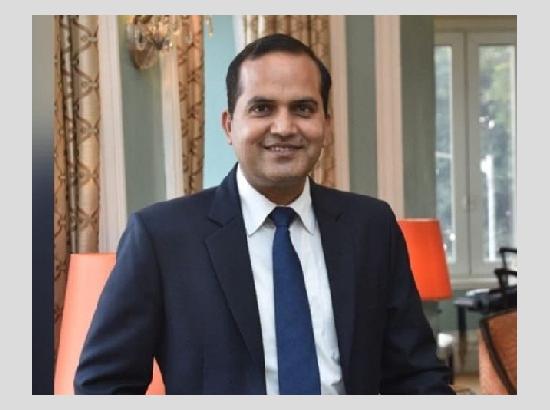
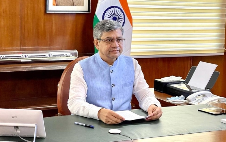
Union Minister of Electronics and Information Technology Ashwini Vaishnaw on Wednesday said that India’s semiconductor mission is focused on talent development and designing the entire chip. In just 24 months or so, India has tied up with 104 universities, redesigned the entire course curriculum, and tied up with international institutions including the University of Purdue to give the semiconductor mission a big boost.
Speaking at the World Economic Forum annual meeting, Vaishnaw said, “The biggest priority is on design that’s where we have a very big strength. We have as I said about 300,000 design engineers. In design, we are advancing from being a back office to actually producing the complete chip or rather designing the complete chip, two going out to the customers taking the concept and then developing the entire chip. So that’s a very important journey. So this is a very big focus for us.”
“The second big focus for us is to make sure that talent for all parts of the ecosystem gets developed and in that, it’s very important to continuously upgrade the course curriculums. It is very important to make sure that we are connected with the companies that are working on it. For example, in applied materials, we’ve worked with them and they have approved a USD 300 investment in India, where they have set up a big base where they’re designing the equipment and that’s an important point for ASML also. They are designing the equipment, and manufacturing the components there so that their supply chain also becomes resilient. So there is a lot of collaboration. There’s a collaboration with another company where they have set up their most advanced training system called ‘Semiverse’ which will be used to train about 6,000 technicians in India in semiconductor manufacturing. So those kinds of collaboration are what we are focussed on.”
Vaishnaw called India the right place for developing semiconductors as the country has a large pool of talent, which includes close to 300,000 design engineers who practically design every complex chip which is manufactured in the world. He said India is looking to develop the complete ecosystem of semiconductors, including design capabilities and manufacturing software and hardware part of it.
Speaking about India’s semiconductor mission, Ashwini Vaishnaw said, “We look at this semi-conductor mission. We call it India Semiconductor’s mission in a very comprehensive way. We know this is a very important industry, and India is the right place for developing it because we have a very large pool of talent already there, with close to 300,000 design engineers designing practically every complex chip that is manufactured in the world. So, it is very natural to move on to the value chain and move towards manufacturing. So, we are looking at developing the complete ecosystem of semiconductors, which means design capabilities, the software part of it, manufacturing the hardware part of it and talent.”
He further said that India, in its semiconductor program has announced and committed to developing 85,000 talents, which includes engineers, BTech, MTech, PhD and technicians for managing clean rooms, working out machines, the entire thing, and the entire spectrum over the next ten years and within a short time. He said, “So, all the experts that we have been discussing with, they say that the entire semiconductor market has evolved in a very interesting way. There is a huge market share and huge demand for chips, which are not on that 7 nanometres, 2 nanometres, kind of cutting edge technologies.”
“There is a significant demand for 28 nanometres and above for automotive, for telecom, for power, for power electronics, for train sets, for everything that goes in the day-to-day household units. At this point, we are focused on getting into that market segment. Once the ecosystem starts developing, then we move on to more leading edges,” he added.
Calling trust India’s biggest capital, he said the entire world has developed a “very big amount of trust” in India. He stated that India has signed a Memorandum of Cooperation with US, Europe and Japan. He further said that India is working with the South Korean government and companies on semiconductors.
Speaking about where New Delhi stands amid the battle between the West and China over chips, the minister said, “If you look at how India has conducted its foreign policy, its economic policy, the way it has conducted itself – the entire world has developed a very big amount of trust on India. That trust is what is our biggest capital. That trust gels the entire world in a very harmonious way. For eg, we have signed a Memorandum of Cooperation with the US, Europe, and Japan.
“On semiconductors, we are working with the South Korean government and South Korean companies. It’s like every possible company wants to collaborate with India in one way or the other. So, we don’t think that it’s a battle, we think that there is enough for everybody. It’s a question of how much importance we give and how much talent we put into it and how much focused we are on it,” he added.
Speaking about how dynamic the semiconductor industry is, he said it is not easy to predict what changes will happen in the next 10 years. He said, “It’s too complex and too dynamic and too uncertain for anyone to bet that this is how the sector will be in 10 years from now.”
He further said, “Just say, how five years back nobody thought that 28-nanometre or 40-nanometre chips would not be viable anymore but the way that the electric vehicle industry has evolved, the way the telecom has become pervasive, those legacy nodes as they were called have become very important market share.”
He said, “We announced this policy in January 2022. It’s just 24 months now and within this short time frame, we have tied up with 104 universities, redesigned the entire course curriculum, and tied up with international institutions including the University of Purdue. We have had the first plant, which was announced during Prime Minister Modi’s US State visit on June 23. And within 90 days of that announcement, the construction of the first plant started in September 2023. So, it’s a very rapid progress, very focused. Yes, unlike the US, which has USD 55 million, our program is at this point of time USD 10 billion.”
Highlighting the change in the semiconductor market, the Minister said that there is a huge market share and demand for chips that are not only 7 or 2 nanometres but also 28 nanometres.


